
Die attach and adhesive deposits
Small adhesive patterns are developed around the bonding area and placement step. Valve, positive-displacement or suitable jetting methods are evaluated for deposit formation with the intended material.
Semiconductor manufacturing
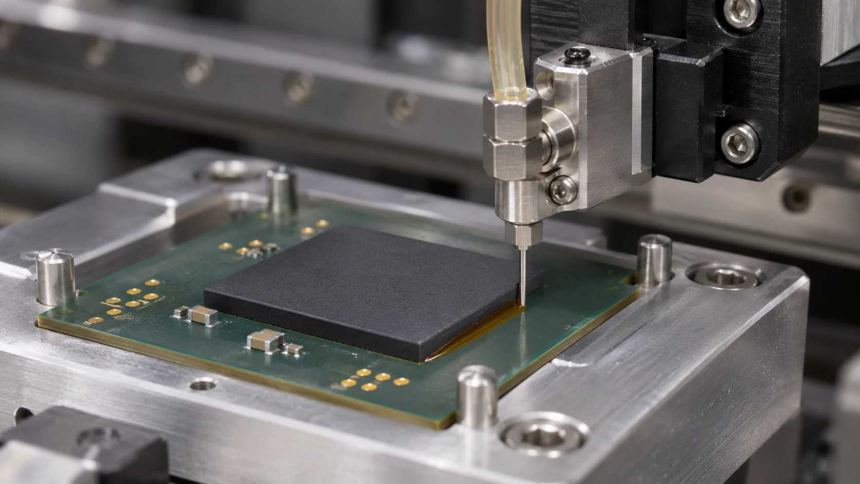
Controlled material placement at the die, package and substrate. LinkTech develops dispensing equipment for adhesive attachment, capillary underfill and local protection, with application trials defining the process.
Industry applications
Die attach, underfill and encapsulation place material in different locations and at different stages of package assembly. The dispense method needs to suit the formulation, the substrate and the available clearance. We evaluate the material delivery and part handling together, with nozzle access, temperature conditions and cure sequence included in the development.
Small adhesive patterns are developed around the bonding area and placement step. Valve, positive-displacement or suitable jetting methods are evaluated for deposit formation with the intended material.
Package-edge dispensing supports capillary flow beneath suitable devices. Glob-top and wire-bond protection require different coverage and flow conditions, so their deposit patterns are developed separately.
Fixtures, fiducial referencing and programmed motion are coordinated with dispensing and curing. Wafer-level tasks are assessed separately for substrate handling, material compatibility and the required equipment environment.
Application development
Process capability is established with the intended package, substrate and fluid. Free testing supports the equipment recommendation; dispense size and positioning requirements are defined for the individual application.
Applications, materials & equipment
Discuss your application with our engineers. We handle the technical evaluation with you.